

WWW.LIVESCIENCE.COM
'This is the next jump in technology': World's first sub-1nm chip keeps Moore's Law alive a little longer
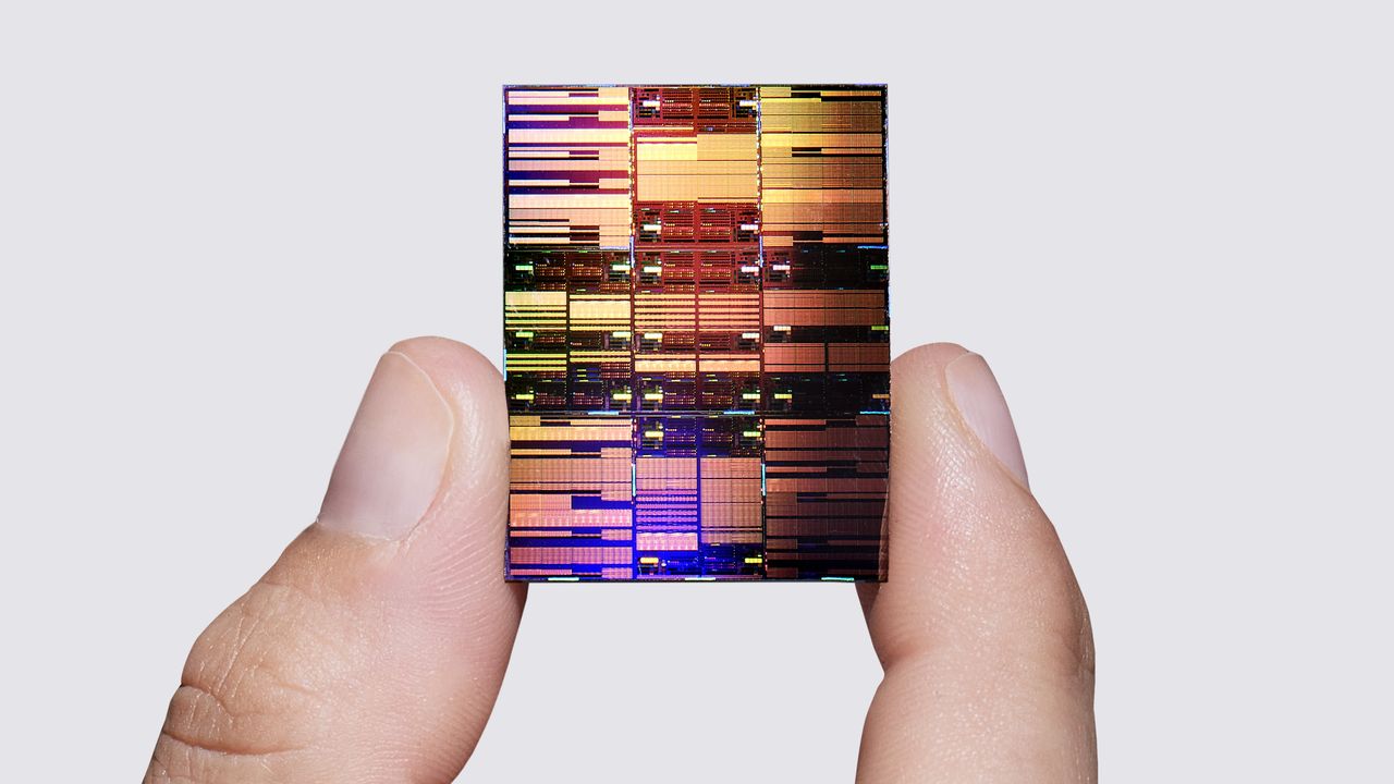
For the first time, scientists can develop computer chips with transistors smaller than 1 nanometer. The new "NanoStack" architecture that has made this possible could even one day lead to transistors as small as 0.1 nm, the scientists claimed. The new 0.7 nm transistors are significantly smaller than those that feature in standard 2 nm semiconductor chips used in supercomputers, AI systems and advanced graphics processing units (GPUs). While size designation doesn't necessarily correlate with an exact measurement of the transistors on the chips, it does represent their general capabilities. Essentially, the smaller the transistors and their supporting components, the more you can fit on a chip. A typical 2 nm chip design, for example, can fit roughly 50 billion transistors onto a space the size of a human fingernail. The new chip features transistors that are so diminutive they're not measured in nanometers but "angstroms," a unit of measurement typically reserved for atoms. The first of these chips is expected to be manufactured with transistors that are a mere 7 angstroms equivalent to 0.7 nanometers or roughly the width of a glucose molecule. At this size, engineers can squeeze nearly 100 billion transistors into a fingernail-size space nearly twice that of the current 2 nm platform.Stacking and staggeringThe scientists achieved this feat using a novel technique called "nanostacking," which they first outlined in a study published as part of the peer-reviewed 2025 Symposium on VLSI Technology and Circuits and uploaded July 2025 to the IEEE Xplore server. This enables engineers to vertically stack the nanosheets used to build the previous generation of 2 nm computer chips.The technology used in all conventional circuits known as complementary metal-oxide-semiconductor (CMOS) demands extremely high temperatures during manufacturing. As transistors shrink, they also suffer from issues such as "charge trapping" where electrons or holes become immobilized by defects or impurities and "gate leakage" static power dissipation. Such problems have posed a challenge to attempts to shrink transistor size below 2 nm, and thus improve the performance and efficiency of computer chips beyond today's best capabilities. IBM's three-dimensional stacked architecture, however, aims to alleviate some of these pain points, the scientists said."NanoStack is nanosheets transistors stacking on top of each other. But it's not through a simple monolithic lithography and etch process," said Huiming Bu vice president for IBM semiconductors global R&D and Albany operations, during a press briefing. "What happens here is we actually stack the device. I call it stacking, but also staggering. Stacking in vertical direction, so the front side of each transistor and the backside of each transistor can be contacted independently for signal and power. The stacking of these transistors are done by single dielectric bonding, which is a key innovation that we have developed." (Image credit: IBM)IBM representatives added in the briefing that the new technology provides up to 50% greater performance with a 70% reduction in energy use versus the 2 nm platform and will eventually replace this technology altogether within the next five years. The scientists say the research could carry deep implications for the computing industry, with revolutionary impacts on the artificial intelligence (AI) and quantum computing sectors. One of the immediate technological benefits could also lie in creating better static random access memory (SRAM) chips, which are used for a variety of computing applications, including CPU caching, networking and in devices such as pacemakers and vehicle sensors. SRAM is also vital in AI processing because it's located close to processing cores (versus other kinds of RAM modules that are often separate components), increasing the speed of data shuttling around systems and therefore reducing bottlenecks.IBM representatives added in the press briefing that they demonstrated a 40% improvement in the scaling of SRAM memory versus the 2 nm platform. This will be a boon to AI workflows, which demand much higher bandwidth and efficiency.The future of computing "We actually have entered a domain that semiconductor manufacturing is almost magic," Huiming added about the design process. "Think about the structure we are building here. We actually deposit the layer atom by atom, and we actually layer atom by atom."IBM representatives said the nanostacking approach isn't a minor upgrade but a generational shift that will eventually enable foundries to scale these chips from 0.7 nm transistors all the way to a single angstrom or just 0.1 nm keeping Moore's Law alive for a little longer at least. Shrinking the transistor nodes on these chips will allow for more powerful processes, they said, thanks to a near-twice jump in the transistor count, while the stacked and staggered design significantly reduces the energy requirements. Huiming said that while everybody demands performance, nobody wants to pay the bill for the power. "It will replace nanosheet as today's mainstream [platform] at leading foundries. Whether it's CPU or GPU," he added. "And we believe that transition will happen at around 7 angstroms. So within a decade, this will become another mainstream [platform] that we have invented. This is the next jump in technology."Related storiesMicrosoft breakthrough could reduce errors in quantum computers by 1,000 timesQuantum internet inches closer thanks to new chip it helps beam quantum signals over real-world fiber-optic cablesScientists trained an AI model using an IBM quantum computer and it answered questions correctly that the base model couldn'tThe findings of the 2025 study suggest that not only can the chipset provide much-improved performance with much lower energy consumption, but it may also provide a path toward reducing the thermal impact that high-power computing has on hardware. These innovations could also have an impact on quantum computing, IBM representatives said, as they could lead to improvements in the classical systems with which quantum computers will work together as the technology emerges. "For quantum computing, we need to use lots of classical compute with it," Jay Gambetta, IBM's director of research, said during the press conference. "We want to build decoders, we want to build controllers for decoders and accelerators. And we are working right now on that type of classical with the 2 nm [platform]. If we can continue to change the platform, use more efficient, more powerful [chipsets], it will only help the rate and pace at which we've got to build the classical compute that goes along with the quantum."
0 Commenti
0 condivisioni
10 Views